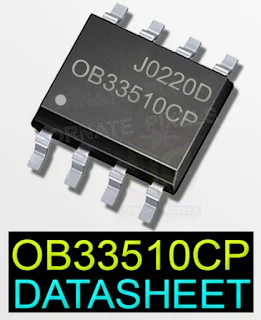
OB33510CP IC or 0B33510CP IC Schematic Circuit Diagram Datasheet (Pinout)
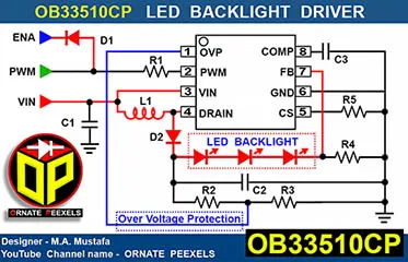
Application- LED Driver of LCD TV / LCD Monitor. OB33510CP IC is mainly used in LED driver circuits. LED TV LCD TVs and flat panel displays have this LED driver circuit. A pulse width module or PWM to Analog dimming mode is available in OB33510CP IC. OB33510CP IC Datasheet Pinout & Schematic Circuit Diagram OB33510CP IC has an over-voltage protection circuit and a current sensor circuit to prevent the backlight LEDs from getting damaged due to overvoltage and over-current. Moreover, the 0833510CP IC has an under-voltage lockout or UVLO circuit and a thermal shutdown circuit for overheating.
The OB33510CP IC has a built-in 100-volt power MOSFET for amplifying weak pulses. The operating voltage or input voltage range of the OB33510CP IC is 9 volts to 30 volts.
This 8-pin OB33510CP SMD IC is widely used in LED LCD TV combo boards because the LED driver circuit made with this IC requires very few components, and the performance of the OB33510CP IC is excellent.
OB33510CP Schematic Circuit Diagram With Pinout Data
 |
OB33510CP IC Schematic Circuit Diagram |
OB33510CP IC Pinout and pins function
How to make VGH VGL AVDD VCOM Module Using NE555 IC?PIN 2 - PWM or Pulse Width Modulation: The brightness of the LED TV's backlight is controlled by this circuit located in OB33510CP IC. This circuit of the IC is governed by the processor IC of the LED TV.
PIN 1 - OVP stands for Over Voltage Protection. This part of the IC monitors the current flowing through the LED through R2 and R3. If the VIN voltage rises or the current flows through the backlight LED beyond the threshold for some other reason, the IC's OVP circuit is activated. It immediately resets the PWM signal so as not to damage the backlight LEDs.
PIN 3 - VIN or Voltage Input, a power supply of 9V to 30V is applied to the VIN pin of the OB33510CP IC.
PIN 4 - Drain There is a MOSFET inside the OB33510CP IC, and the drain terminal of that MOSFET is directly connected to pin number 4. The forward bias voltage is supplied to this drain through the converter output Inductor, and from here, the voltage is output - for the backlight LED
PIN 5 - CS or Current Sense. This terminal is connected to the IC's current sense amplifier and a ramp adjustment circuit.
PIN 6 - GND This is the Ground pin
PIN 7 - FB stands for feedback. The current of the backlight LED is fed back to this pin of the OB33510CP IC to control the output voltage.
PIN 8 - COMP (Compensation) - This is the boost converter loop compensation terminal.
This COMP circuit controls the output circuit current based on the type of load used.
Sony Bravia Smart TV Red Light Blinking 2-Times? Click Here
So far, I am still looking for an IC compatible with OB33510CP IC in any LED TV or monitor; if I find any substitute IC for OB33510CP IC in any LED TV board, I will update that information here.
SM4186 T-Con with DC to DC Converter IC Data - CLICK HER


2 comments:
আমি কি আপনার মোবাইল নাম্বারটি পেতে পারি , আমার একটি ৪২ ইন্চি নন ব্রান্ড স্ম্রাট টিভি আছে , ছবি আসেনা কথা আসে ।
Very usefull information about BL Driver.
Post a Comment