10.8.24

SM4151 IC Circuit Diagram Datasheet

SM4151 IC schematic circuit diagram datasheet and Pinout. This IC is used for all power management of LCD panels, in which DC-to-DC converter and level shifter circuits are integrated.

This IC does not have pins; it has 48 terminals in the QFN package. Moreover, the SM4151 IC has a metal pad at the bottom, which is connected to the ground and acts as a heat sink.

SM4151 IC Schematic Circuit Diagram

The circuit diagram of the SM4151 IC is published below; from pin (terminal) 30 to pin 36 of the IC, six CKV, and STV are output from these six pins.

Moreover, the SM4151 IC has three voltage boost converters, from which the AVDD, VON, and HVDD boost voltages are output, and the VSS and VOFF voltages are output from the buck converters belonging to this IC.

The LCD panel of Sony Bravia Smart TV is installed with SM4151 IC, which is used in DC-to-DC converter and logic level shifter circuits.

The operating voltage of the SM4151 IC ranges from 9.5 volts to 14 volts. Because this IC can be damaged if a short circuit occurs in the LCD panel, it has a system of short circuit protection, overload protection, and thermal protection.

SM4151 IC Circuit Diagram

SM4151 IC Schematic Circuit Diagram and Datasheet
SM4151 IC Schematic Circuit Diagram & Pinout Data

Output and Input Voltages of SM4151 IC Circuit

VIN +12 Volts, VLOGIC (VCC) +3.3 Volts, AVDD +15 Volts, VON +28 Volts, VSS-6.5 Volts, VOFF -12 Volts. VCOM +7 Volts, CVO +7 Volts.

SM4151 IC Equivalent or Substitution

I noticed no difference between the circuit diagram of SM4151 IC and RT6906B IC; the operating voltage and output voltage of both ICs are the same.

Moreover, the pin configuration and package type of SM4151 IC and RT6906 IC are the same. So, RT6906 IC is the substitute or equivalent of SM4151 IC.

SM4151 IC Datasheet Pinout PDF

The SM4151 IC datasheet and pinout are not published on this page in PDF format, but the circuit diagram of the SM4151 IC above shows the pinout data and pin configuration.

5.7.24

Functions of AVDD STV VGL VCOM VGH

What are AVDD, STV, VGH, VCOM, VGL, and CKV, and what are their functions? To understand these things, you need to know some basics of LCD panels first. We try to understand those aspects of the LCD panel. A tiny liquid crystal cell is below the RGB subpixels of the LCD panel and above the backlight (Look at the diagram).

When these crystal cells are energized, the molecular position of the Liquid crystal changes, and when De-energized, the molecules return to their normal orientation. During this process, the crystal cells act as a light barrier. When the crystal cells become entirely black, the backlight's light cannot reach the bottom of the pixels. Thus, the liquid crystals block the light waves and control the brightness of the pixels by opening the light path as needed.

This liquid crystal cell has two electrodes, one of which supplies a negative voltage VCOM, the positive voltage is provided to the other terminal by the source terminal of the thin film transistor (TFT), and the AVDD voltage is supplied to the drain of this TFT. Moreover, VGH or VGL voltage is provided to the gate terminal of the TFT at a specific time to make each TFT active, semi-active, inactive, etc.

What is AVDD, & what is its function in LCD and LED Display

AVDD stands for Analog Voltage for Drain-to-Drain, which some call an Analog power supply. Other names of AVDD are VDDA, HVAA, VSA. Each subpixel of the LCD receives a polarized light wave from the backlight, and there is a liquid crystal cell between the backlight and the subpixel to control the polarized light.

Functions of AVDD STV VGL VCOM VGH

What is VGH, STV, AVDD, VGL, VCOM in LCD or LED TV or Monitor

To control the brightness of the sub-pixels according to the screen image, it is necessary to supply variable voltage to the two electrodes of this liquid crystal cell. A negative voltage is supplied to one electrode of the liquid crystal cell, and a positive voltage is provided to the other electrode by the source terminal of a thin film transistor. AVDD is supplied to the drain terminal of that TFT.

What is VGH in LCD, and what is its function?

The VGH is the acronym for Voltage High Gate, which is the boost voltage generated from the DC-to-DC converter. Its other name is VON / VGON/ VDDG. The VGH circuit in LCD has 20V to 33V and requires a 50mA current. An LCD panel comprises liquid crystal cells associated with thin-film transistors (TFTs).

These TFTs are responsible for adequately controlling the activity of the liquid crystal cells. To operate the TFT, a reverse bias voltage is applied to its gate terminal through gate COF; the source of that reverse bias voltage is VGH or High Gate Voltage.

What is VGL, and what is its function?

The complete form of VGL is a voltage high gate, which is the minus voltage generated by the DC-to-DC buck converter. Other names for VGL are VOFF, VGOFF, and VEEG. The voltage range of VGL is -5 volts to -10 volts, and the current is 100mA.

In an LCD (Liquid Crystal Display) panel, VGL, which stands for "Voltage Gate Low," is a voltage used to control the operation of thin-film transistors (TFTs) on the display. The TFTs are an essential component of an LCD panel as they act as individual pixel switches, allowing or blocking the passage of light through each pixel. VGL is responsible for controlling the "gate" of these transistors.

What is a AAA Super AMOLED Display?

What is VCOM, and what is its function in LCD/LED Display?

VCOM is the Common reference voltage for each sub-pixel of the LCD panel. A tiny liquid crystal cell is placed under each subpixel to make the pixels of the LCD panel active or bright and dim. The number of these liquid crystal cells is several billion in an LCD.

Each liquid crystal cell has two electrodes; if we call one of these electrodes a cathode and the other an anode, positive voltage is supplied to the anode, and negative voltage is provided to the cathode. In this case, the cathodes of all the crystal cells of the LCD are connected by a conductive print, and a negative voltage is supplied.

Then, indeed, we understood that the cathode terminals of the liquid crystal cell are marked as Common. VCOM, or Common voltage, is applied to these Common terminals. VCOM stands for Common Voltage, through which liquid crystal cells receive negative voltage.

What is STV in the concept of LCD?

STV is a Vertical Sync Input pulse. It determines the time to produce the next frame after a one-frame scan to make the image. When the rising edge of STV occurs, it marks the beginning of a data frame. The STV input is also used to generate the high-voltage STV or Start Pulse Output.

This high-voltage output is low (connected to VGL) whenever STV is low, and it becomes high (connected to VGH) only when STV is high and both CPV and OE are low.
What is CKV, and what is its function? Click here

7.6.24

SM4053C IC Circuit Diagram Datasheet Pinout and Voltage Details

 SM4053C IC contains one buck converter for VGL output and three boost converters for VDD, HVDD, and VGH output. This multi-function IC has several DC-to-DC converters, gamma, logic level shifters, and VCOM sections. Moreover, SM4053C IC provides overload-protected VGH ODD and EVEN output with a flip-flop technique.

Application- Power management of LCD TV and LCD Monitor display panel
Package- QFN Quad flat no-lead package
Number of terminals - 14x4 = 56
Operating Voltage VIN -  DC 9.4 Volts to 14 Volts
Logic Voltage (Vlogic) - 3.3 Volts

Protection - Excellent protection against over-voltage, short circuit, over-current, and over-temperature events is provided by the SM4053 IC, which protects the LCD panel.

The output voltages of SM4053 IC - VDD 15 Volts, HVDD - 7.5 Volts, VGL- -5 Volts, VGH- 27 Volts.
CLK1, CLK2, CLK3, CLK4, CLK5, and CLK6 are usually 7 volts.
Gamma output voltages are different voltages for different displays.
The flip-flop voltages of VGH ODD and EVEN are sequentially -5V and +27V.

SM4186 IC Pinout Diagram HERE

SM4053C IC Schematic Circuit Diagram Datasheet and Voltage Details

The circuit diagram of the SM4053C IC includes the datasheet and pinout of the 3NP and 3PN components marked Q1 and Q2. 3NP or NSM80101MT1G is an NPN Transistor with a Series Switching Diode, and 3PN or NSM80100MT1G is a PNP Transistor with a Series Switching Diode. Here Q1 is 3NP, and Q2 is 3PN

Schematic circuit diagram SM4053C IC with pinout
SM4053C IC Circuit Diagram and 3PN and 3NP Pinout Pin data

3PN  and 3NP Datasheet of SM4053C Circuit

3PN or NSM80101MT1G Datasheet -

PIN PINOUT
1 CATHODE
2 BASE
3COLLECTOR
4 ANODE
5 C & A
6 CATHODE

Pin1- Cathode and anode of two diodes, Pin2 - Base of Switching Transistor, Pin3- Collector, Pin4- Emitter, Pin5- Anode of Switching Diode, Pin6- Cathode of Switching Diode.

RT6908 IC Schematic Circuit Diagram Here

3NP or NSM80101MT1G Datasheet-

PIN PINOUT
1 EMITTER
2 BASE
3 C AND A
4 ANODE
5 CATHODE
6 CATHODE

Pin1- Emitter of Switching Transistor, Pin2 - Base, Pin3- Anode and Kathode, Pin4- Anode, Pin5- Kathode, Pin6- Collector of Switching Transistor.

SM4053C IC Substitution information, components list, and values:

TPS65175 IC is equivalent to SM4053 IC. Both IC circuit diagrams' component lists and values are published here.

2.6.24

TPS65175 IC Circuit Diagram Pinout & Substitution

TPS65175C IC is an integrated circuit designed by Texas Instruments. It is a power management IC commonly used in LCD panels, especially applications requiring multiple power rails. The IC is part of the TPS651xx family, known for its versatility and efficiency in managing power.

Here are some key features and functions and the circuit diagram of the TPS65175 IC:

Wide Input Voltage Range: TPS65175 IC is used in the power management circuit of LCD panels of LCD TVs, desktop monitors, etc., providing flexibility in various applications.

High Efficiency: The internal circuit of TPS65175 IC is designed for high efficiency, helping to optimize system power consumption.

Protection Features: The TPS65175 IC has built-in thermal shutdown and over-current protection, which is excellent for protecting the LCD panel.

Application: The TPS65175 IC is used in the power management circuit of LCD panels in LCD TVs and desktop monitors. It is also used in the E15063094V-0 T-Con board, which is installed in Philips, Videocon, and Walton LCD TVs.

Multiple Outputs: The IC can provide multiple regulated outputs, making it suitable for systems that require different voltage levels.

Low-Dropout Regulators (LDOs): The TPS65175 IC has a VGH boost converter and a VGL buck converter, which are controlled by low-dropout VGH and VGL charge pump regulators.

TPS65175C IC Schematic Circuit Diagram and Datasheet / Pinout


TPS65175 IC Schematic Circuit Diagram and datasheet

TPS65175 IC Schematic Circuit Diagram & Pinout

Components List & its Values of TPS65175 IC's Circuit Diagram:

 L1 - 220µH, L2 - 220µH, L3 - 470µH SMD, FU1 - 6 Amp SMD Fuse.

C50 - 0.22µF, C51 - 0.22µF, C53 - 10µF, C54 - 0.1µF, C1 - 0.33µF, C2 - 0.01µF, C69 - 0.1µF, C70 - 4.7µF, C71 - 4.7µF, C72 - 4.7µF,

C60 - 3.3µF, C61 - 3.3 µF, C62 - 2.2µF, C64 - 01.µF, C114 - 0.1µF, C80 - 0.1, C81 - 2.2µF, C82 - 2.2µF, C110 - 22µF, C12 - 22µF, C13 - 22µF, C40 - 0.2µF, C41 - 0.2µF, C41 - .02µF, C42 - 4.7µF.

R1 - 0Ω, R2 - 33KΩ, R31,32,33,34,35,36 - 1Ω, R46 - 3.6KΩ, R50 - 82KΩ, R51 - 33KΩ, R52 - 0Ω, R123 - 0Ω, R63 -0Ω, R64 - 9.1KΩ, R90 - 18KΩ, R71 - 5.1KΩ.

D2, D1 - 315A, Q1 - 3PN (Integrated PNP Transistor and two diodes), Q2 - 3NP - Integrated NPN Transistor and two diodes)

TPS65175 IC Substitution or equivalent:

The substitution of the TPS65175 IC can be SM4053C IC because either of the TPS65175 and SM4053C ICs are used on the E15063094V-0 T-Con board.

Components List & its Values of TPS65175 IC's Circuit Diagram

L1 - 220µH, L2 - 220µH, L3 - 470µH SMD, FU1 - 6 Amp SMD Fuse.
C50 - 0.22µF, C51 - 0.22µF, C53 - 10µF, C54 - 0.1µF, C1 - 0.33µF, C2 - 0.01µF, C69 - 0.1µF, C70 - 4.7µF, C71 - 4.7µF, C72 - 4.7µF, C60 - 3.3µF, C61 - 3.3 µF, C62 - 2.2µF, C64 - 01.µF, C114 - 0.1µF, C80 - 0.1µF, C81 - 2.2µF, C82 - 2.2µF, C110 - 22µF, C12 - 22µF, C13 - 22µF, C40 - 0.2µF, C41 - 0.2µF, C41 - .02µF, C42 - 4.7µF.

R1 - 0Ω, R2 - 33KΩ, R31,32,33,34,35,36 - 1Ω, R46 - 3.6KΩ, R50 - 82KΩ, R51 - 33KΩ, R52 - 0Ω, R123 - 0Ω, R63 - 0Ω, R64 - 9.1KΩ, R90 - 18KΩ, R71 - 5.1KΩ.

D2, D1 - 315A
Q1 - 3PN (Integrated PNP Transistor and two diodes)
Q2 - 3NP (Integrated NPN Transistor and two diodes)

TPS65175 IC Substitution or equivalent

The substitution of  TPS65175 IC can be SM4053C IC, as the T-Con board of the  E15063094V-0 model uses both TPS65175 IC and SM4053C IC.


31.5.24

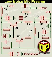
Low Noise Microphone Preamplifier Circuit Diagram

Microphone Preamplifier Circuit Diagram using Transistor: To get crystal clear sound from the loudspeaker, we need a high-performance microphone preamplifier module capable of receiving and outputting all signals in the audio frequency range of 20Hz to 20KHz.

Here is the circuit diagram of the microphone preamplifier, which can provide low-noise audio signal output for condenser/electret microphones or dynamic microphones.

Low Noise Microphone Preamplifier Schematic Circuit Diagram

This microphone preamplifier circuit is suitable for dynamic microphones of 600Ω to 1KΩ impedance and will also provide excellent performance for condenser microphones.  Refer to the complete guidelines to build this microphone preamplifier board according to your requirements.

Microphone preamplifier circuit diagram for condenser and dynamic microphone
Microphone Preamplifier Circuit Diagram 

Components Value For Mic Preamplifier Circuit-

TR1, and TR2 - BC547 or C2120 NPN Transistor, D1 - 8.2 Volt Zener Diode.

R1 - 4.7KΩ, R2 - 100KΩ, R3 - 47Ω, R4 - 56Ω, R5 - 3.3KΩ, R6 - 1KΩ, R7 - 1.5KΩ, R8 - 1KΩ,

R9 - 1KΩ for 12V Circuit, 3.9KΩ for 24V Circuit.

C1 - 1µF, C2 - 220PF, C3 - See below, C4 - 22µF, C5 - 2.2µF, C6 - 220µF, C7 - 330PF

C3 is 10µF for dynamic microphones and does not need to be installed for condenser or electret microphones.

Some Tips for Getting the Best Performance from Microphone Preamplifier Circuits:

• The negative supply of this mic preamp circuit board cannot be taken from the main audio output section; it must be soldered to the front body of the metal cabinet.

• A wire from the ground section of the audio output amplifier circuit should be soldered to the rear of the metal cabinet.

• No ground connection should be provided in the middle of the cabinet.

• The ground connections of the microphone socket should be connected very close to the input section of the mic preamp circuit.

• A mic preamp circuit board should be placed in the front of the cabinet, and the audio output amplifier board or components and power transformer should be placed on the backside.

Powered by Blogger.
Youtube Channel Image
Ornate Pixels On YouTube Subscribe to Ornate Pixels
SUBSCRIBE