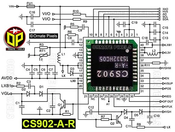
The CS902-A-R IC is used in the DC-TO-DC converter circuit in the TCL LCD panel's power management circuit. Inside the CS902 IC, N-channel and P-channel MOSFETs for boost and buck converter circuits are integrated.
In the circuit diagram of CS902 IC, the VIN terminal is the voltage input terminal, where 12 volts is usually input as the operating voltage. The CS902-A-R IC is a programmable TFT LCD power management IC (PMIC). In the circuit diagram, the SCL and SDA signals connect to pins 5 and 6 of this IC, which are coming from the processor. Data and clock pulses can control the output voltage of the CS902 IC circuit.
The MT3151A05-5XC-5 T-Con circuit board uses CS902-A-R or CS902 IC as a DC-to-DC converter or LCD power management IC (PMIC). CS902 IC is also installed on the MT3151A05-9-XC-2 T-Con circuit board.
CS902-A-R IC Schematic Circuit Diagram
As per the size and voltage requirements of TFT (Thin Film Transistor) LCD TVs and monitors, the CS902 IC schematic circuit diagram design may vary slightly, keeping the basics right.
CS902-A-R IC Schematic Circuit Diafram
 |
| CS902 DC-to-DC IC Schematic Circuit Diagram |
Component Valu of CS902-A-R IC Circuit Diagram
Capacitors: C1- 10µF, C2-0.22µF, C3-0.47µF, C4- 10µF, C5- 10µF, C6- 10µF, C7- 10µF, C8- 1µF, C9- 470pF, C10- 10µF, C11- 1µF, C12- 0.22µF, C13- 10µF, C14- 10µF, C15- 10µF, C16- 22µF, C17- 10µF, C18-0.1µF, C19- 10µF.
Resistors Value: R1 10KΩ, R2- 2.2Ω, R3- 22KΩ, R4- Unknone, R5- 75KΩ, R6- 51KΩ, R7- 10KΩ, R8- 2.2Ω, R9- 4.7KΩ, R10- 4.7KΩ, R11- 1KΩ.
Inductors and Fuse Value: F1- 6Amp, L1- 100µH, L2- 6.8µH
Values of Transistors in CS902 IC Circuit Diagram:
Q1 - NPN Transistor, Q2 - S2A (PNP Transistor)
Diodes Values in CS902 Diagram:
SMD Diode - It will be updated
Output & Input Voltages details of CS902 IC Circuit
• VIN—Depending on the circuit design, the operating voltage of the CS902 IC ranges from 8 volts to a maximum of 14 volts.
• Logic Voltage - 3.3 Volts
• VGH - 20 volts to 40 volts output as VGH from positive charge pump regulator (programmable)
• VGL - Can output -4.5 volts to -13 volts as VGL from a negative charge pump regulator (programmable).
• AVDD—The output from the sync-boost regulator of the CS902 IC circuit ranges from 13.5 volts to 19.8 (by programming).
P301-16 IC Schematic Circuit Diagram Here


No comments:
Post a Comment