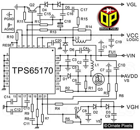
TPS65170 IC Schematic Circuit Diagram Datasheet Pinout and I/O Voltage Details:
The TPS65170 is a power management IC (PMIC) for LCD TVs and monitor display panels. This IC's operating voltage (VIN) is 8.6V to 14.5 volts DC. Note that in the schematic circuit diagram of TPS 65170 IC below,
The operating power supply voltage is applied to pins 27 and 28. TPS65170 IC provides various bias voltage supplies to LCD panels. Before understanding the circuit diagram of the TPS65170 IC, let's take a look at its features.
TPS65170 IC Schematic Circuit Diagram & Feature
• Package: 28-pin QFN package with a dimension of 5x5mm
• Input voltage range of TPS65170 IC: 8.6V to 14.5V
• Switching frequency: 750KHz (fixed) for boost and buck converter
• Switch current limit 1.5A buck converter
• Output voltage: Maximum 18V from main boost converter
• Soft-start programmable boost and buck converter
TPS65178A IC Circuit Diagram Here
• Isolation switch with controlled signal for external high-side MOSFET
• Programmable reset pulse to reset the signal
• TPS65170 IC has an integrated thermal shut-down circuit
• Two regulated charge pump circuits for VGH and VGL outputs
• Short circuit and overload protection
• The feedback (FB) signal circuit for short circuit and overload protection is observed in the circuit diagram of TPS65170 IC.AAA
TPS65170 IC Schematic Circuit Diagram is Below
On the upper left side of the TPS65170 IC circuit diagram, the symbol AGND represents analog ground, and the PGND represents power ground.
 |
| TPS65170 IC Schematic Circuit Diagram |
Component List and its value in TPS65170 IC Circuit
F1- 1.6A 63V SMD fuse
Capacitors-
C1, C2,C3-15.3µF, C4- 0.1µF, C5- 30µF, C6- 10nF, C7- 30µF, C8- 1µF, C9- 10µF, C10- 0.1µF, C11- 0.1µF, C12- 22µF, C13- 0.1µF, C15- 0.1µF, C16- 0.1µF, C17- 0.01µF, C18- 10µF, C19- 44µF.
Resistors-
R1,R2- 100KΩ, R3-15KΩ, R4- 20KΩ, R5- 100KΩ, R6- 2Ω, R7- 1KΩ, R8- 1.3KΩ, R9- 33KΩ, R10- 100KΩ, R11- 100KΩ, R12- 2.2MΩ, R13-2.4KΩ R14- 10Ω.
I/O Voltage Details of TPS65170 IC
• VIN 8.6V to 14.5V
• VGH 26 Volts
• VGL -5 Volts
• AVDD 16 Volts
• VCC 3.3 Volts (Logic)
[ Schematic Circuit Diagram of RT6908 IC ]
Pin Function of TPS65170 IC.
1. VL- Decupling capacitor connection for internal power supply.
2,3. SWB- Buck converter switch node.
4. CTRLN- Base driver signal output for external positive charge pump regulator transistor.
5. FBN- Feedback input for a negative charge pump.
6. FBB- Feedback input for the buck converter.
7. RST- Drain output for reset generator.
8,14. AGND- Analog ground. The symbol for AGND is shown in the TPS65170 IC circuit diagram above.
15. DLY- Delay capacitor connection for the positive charge pump and boost converter.
16. CRST- Timing capacitor connection pin for reset generator.
17. SS- Soft Start, Timing capacitor connection for soft start.
18. COMP- Compensation network connection for the boost converter.
19. FB- Feedback input pin of boost regulator.
20. FBP- Feedback input pin for positive charge pump circuit.
21. CTRLP- Base driver output pin for external positive charge pump regulator transistor.
22. GD- Get driver output pin for external MOSFET.
23,24. Switching node for the boost converter.
25,26. PGND- Power ground. The symbol for PGND is shown in the TPS65170 IC circuit diagram above.
27,28. VIN- Operating voltage input pins.
TPS65170 IC Substitute
TPS65170 IC has been installed in the LCD panel of the LG LCD TV and LG computer monitor. I don't know about the substitution of this IC at the moment. I will update you as soon as I get the information.
TPS65175 IC Schematic Circuit Diagram >> Here
No comments:
Post a Comment